Arm Box PCB V2
Documentation
Sonia Ly
Task Overview
- Modify the design of last year’s Arm Box PCB to include:
- Edge Card connector slots to slot in the new ESC Carrier Boards
- Add a toggle switch to turn on/off the fans
- LED to indicate if an ESC is in or not
- Modify the layout to:
- Make removing and inserting connectors easier
- Change the Top → Bottom order to Elbow → Shoulder → Waist (instead of S → E → W)
PCB Information
- Size: 100x70mm (Same as last year)
Signals coming out of the ESC
5 Power Signals:
- Phases A,B,C, rate for ~20A if possible (3 connections here)
- Power and Ground, rate for ~20A (2 connections here)
12 Data signals:
- 5 Encoder signals: 5V, GND, A, B, Z
- 4 Limit Switch Signals: EXT_INT1, EXT_INT2, GND, GND
- 2 CAN Signals: CAN_H, CAN_L
- GND extra
Choosing an Edge Card Connector
When choosing an Edge Card connector, I made the following assumptions:
- The new ESC Carrier board would be a 4-layer board
- (For reference, JLC PCB’s average 4-layer board thickness is 1.6mm)
- We want the cheapest option possible
- (so getting the connector from Molex would be a big +)
- Ideally, want don’t want a connector that’s too long
- (around the width of an ESC, ~30mm)
The best option I could find that fit most of those criteria was combining the 2 following edge card connectors:
| Type | Guides? | Female (Sonia’s side) | Male right-angled (James’ side) |
|---|---|---|---|
| 4PW + 12SIG | Yes | 461144120 | 459854413 |
| No | 461144121 | ||
| 2PW | Yes | 461120203 Cannot be sampled for free! | 459852932 |
| No | 461120201 |
Useful Links
- Arm Box Board 2025
- Arm Box Board 2026
- Carrier ESC PCB Board 2026 (TDB)
Personal Notes
Changes:
- Make the board longer, horizontally
- Deal with all the CAN changes
- Adjust Layer stack
- Net tie
Changes to be made:
- 4 pos connectors for lim switches
- Extra switch for can termination
- Make the connector that goes to the brushed board on top (consider putting it on the other side)
- Switch phase c is 24 v actually
- Make the fuses more accessible
TODO: DOUBLE CHECK IF CONNECTOR ORIENTATIONS ARE CORRECT(not a concern whoops)- Fan connectors on the side perhaps
- Via to probe gnd
- on/off indicator for switches
- Clean up molex connector sheet
- Adjust layer stack
- Review connector thickness and if it interferes with anything (perhaps just add the 2d model
Modifs to make:
- Go the can stuff on layer 4
- Make
- Change pinouts on connectors to make life easier
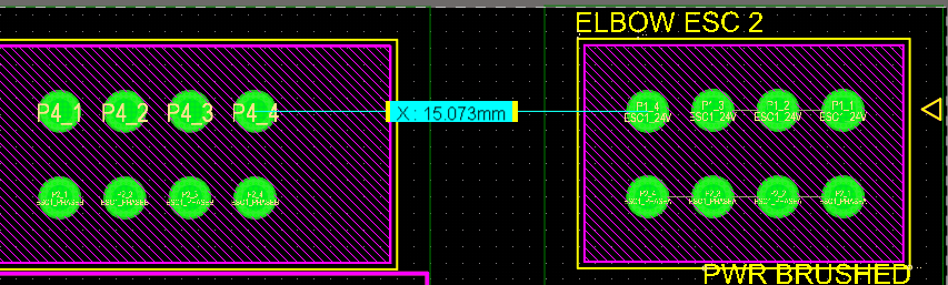
Distance between 2 pins:
Questions:
- Does signal GND always have to be different from power GND? Why?
- Prevent interference?
- Are the limit switches tied to signal gnd or power gnd
- How to implement CAN termination lol
NOTABLE CHANGES TO REPORT:
- Net label change of lim switches